Decades of Experience
i >350 fully custom ICs
b Over 30 years of experience
jOver 15 different silicon foundries
cProcess experience ranging 60nm-1.2um
pInfrared camera development
fTest system development
kApplications
- IR detectors / preamplifiers / multiplexers
- LIDAR detectors & readout
- Laser drivers
- Photonic counting circuits
- Micro-power A/D and D/A converters
- Column parallel to 16-bit resolution (voltage- or time-to-digital)
- In-pixel ADC to 18-bit resolution
- Sigma-delta to 20-bit resolution for linear array
- X-ray and high energy particle detectors and interface chips
- Radiation hard versions of above
- Image sensors (CMOS and CCD)
- Image processors
- Integrated liquid crystal drivers
bChip Size Extremes
- 300um diameter die size imagers for medical applications
- 17×19 mm2 display driver for projection displays
- 51×25 mm2 visible/scintillator x-ray sensor (using stitching)
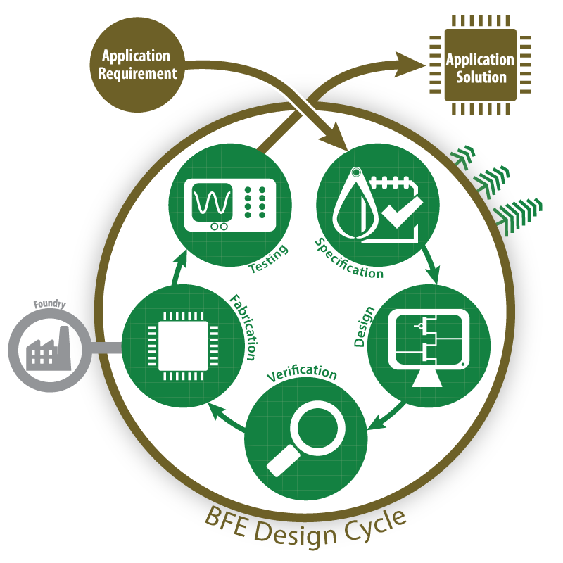
gDesign Types &
- 2Ghz analog bandwidth CMOS for LiDAR range sensing
- TDC (LiDAR)
- Single photon detection
- APD Heterodyne/Geiger/Linear
- 22V CMOS devices
- TDI (Analog / Digital)
- Display / Spatial Light Modulator / LCOS
- Far infrared & high energy particle readout processors
- NIR, SWIR, MWIR, LWIR
- Gamma, X-Ray
- Visible, Low Light
hNon-Standard processes &
Unique & cutting edge applications often require specific technologies
- IR Detectors – InGaAs, QWIP, HgCdTe, SLS, PbSe, a-Si
- Bolometer
- Thermopile – Micrel
- PiN detector – Micron Semiconductor Ltd.
- Rad-hard CMOS – Honeywell 0.8 SOI
- CCD – Supertex 1.2um
jFoundry Experience
- TSMC 0.13um, 0.18um, 0.25um, 0.35um (includes their BCD [Bipolar, CMOS, DMOS] Power management technology)
- Tower/Jazz/TPSCo 65nm, 0.13um, 0.18um, 0.25um, 0.35um, and BiCMOS (Stitching)
- Design Cycle Partner with TowerSemi
- IBM (corp. site) 0.13um
- Austria MicroSystems 0.35um
- Others include: AMIS (0.5um, 1.2um), CSMC (0.6um), Fujitsu (0.25um), HP (0.35um, 0.5um), Amkor (0.35um, 0.5um), Texas Instruments (0.8um, 1um), UMC (0.4um (5V))
jMask Types
- Full Mask Sets
- Stitching: Enables fabrication of large dice. A repeated exposure masking process that has its own complexities yield considerations.
- MPW: In addition to foundry specific multi-project wafer runs we have worked with MOSIS • Global Unichip • EUROPRACTICE.
hProcess Types & Materials
- CMOS
- CMOS/CCD
- Bi-CMOS
- BCD (Bipolar, CMOS, DMOS)
- CMOS-SOS
dDevice Protocols/Interfaces
- SERDES
- USB
- SPI
- LVDS
fCustom Test Systems
Performance built for your specific requirements.
- Wafer probing
- Testing at cryogenic temperatures
- PCB designs and interfaces using FPGA, CPLD and a variety of other components
- Solutions for system interface problems:
- High density interconnect
- Non-standard packaging
- Optics